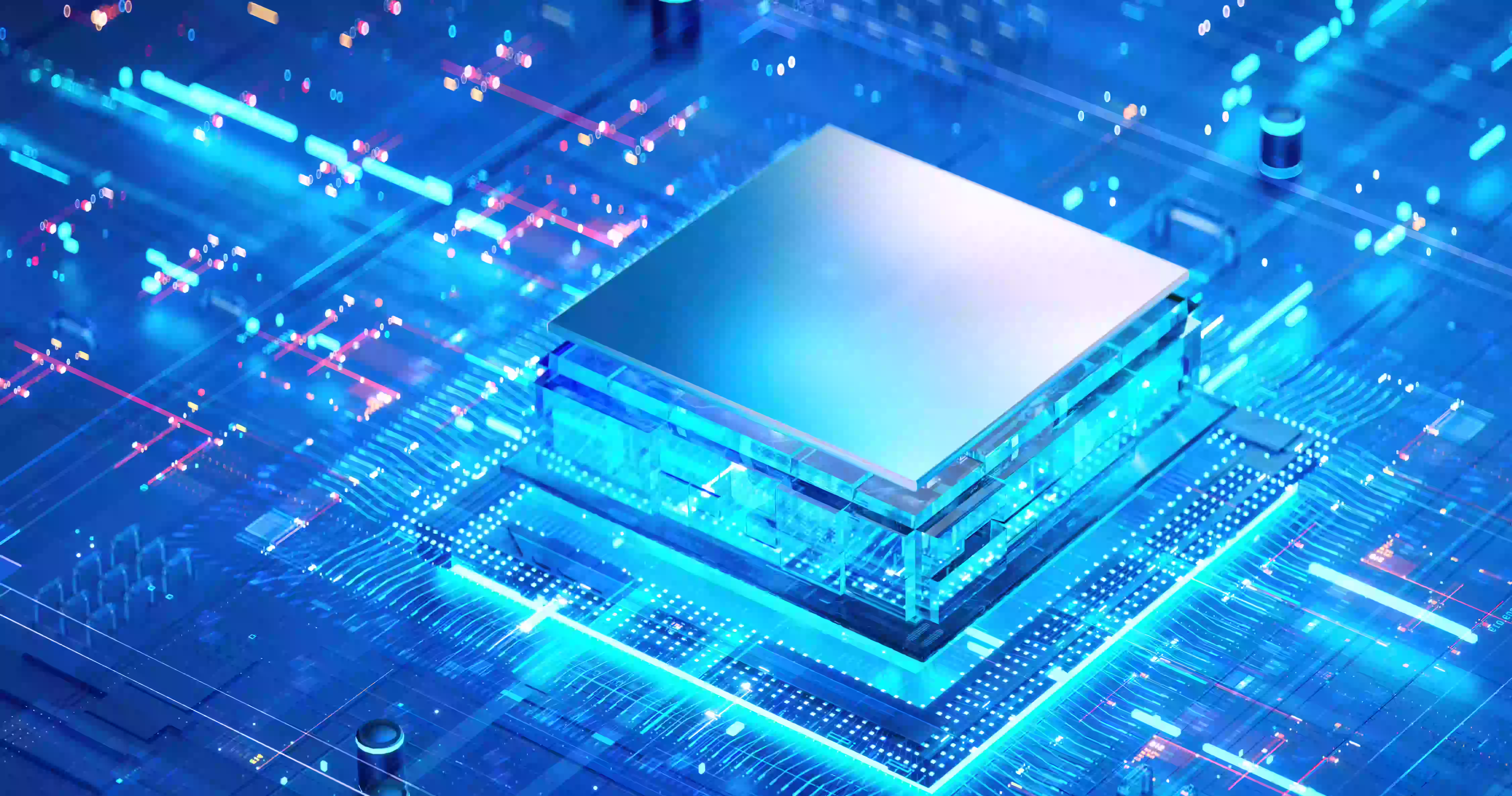
Innovation Beyond the Chip: Exploring Advanced Packaging Architectures
For decades, the semiconductor industry relied on Moore’s Law—the idea that the number of transistors on a chip doubles roughly...
Read MoreInsights from the minds of innovators
For decades, the semiconductor industry relied on Moore’s Law—the idea that the number of transistors on a chip doubles roughly...
Read More
3D NAND memory is pervasive in today’s electronics – mobile devices, laptops, data centers, automobiles, and USB drives are...
Today, KLA Corporation announced our new Surfscan® SP7XP wafer defect inspection system. This new member of our Surfscan family...
As 5G smartphones, advanced automotive electronics, medical and WFH/LFH (learn-from-home) devices become lighter in weight, smaller in form factor...
Every year, Ann Arbor SPARK organizes a series of tech-related events in the Ann Arbor region called a2Tech360. KLA...
Earlier this year we launched KLA Instruments, bringing together many of our product lines in the surface metrology space....
Check out the infographic below to see some of KLA’s key financial information from the 2020 September Quarter, as...
KLA is proud to announce the appointment of MaryBeth Wilkinson as our new executive vice president, chief legal officer...
Enjoy the previously unreleased interviews with KLA’s engineering teams below! The original post follows. Today, KLA Corporation announced the...
Complex, high-volume semiconductor manufacturing processes require advanced optical and EUV reticles. These reticles must be error-free, as reticle defects...
If you are a current KLA Employee, please apply through the KLA Intranet on My Access.